
Precision Solutions for Electronic Materials
Strengthen Your EPSRC Strategic Infrastructure Funding ApplicationGain deeper insights into electronic materials with ZEISS. Let’s discuss how we can support your application.
As transistors continue to shrink, the need for advanced microscopy in electronic materials research has never been greater. ZEISS microscopy solutions empower researchers with cutting-edge capabilities, including non-destructive 3D imaging, AI-driven image analysis, and high-throughput TEM sample preparation. Our instruments deliver multiscale insights into electronic materials, chips, and integrated circuits—helping you push the boundaries of innovation.
Explore our solutions below and get in touch to discuss how ZEISS can strengthen your application.
Case Studies: Advancing Research with ZEISS Microscopy
Discover how our cutting-edge microscopy solutions are driving innovation in electronic materials research.

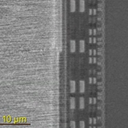
Artificial Intelligence (AI) segmentation of a Silicone Carbide (SiC) Metal–Oxide–Semiconductor Field-Effect Transistor (MOSFET)
3D imaging of SiC MOSFET power device architecture and dopant regions can be performed by FIB-SEM tomography using 30 kV Ga-FIB and an in-column detector sensitive to low-energy SE. However, manual or conventional automatic segmentation of such data to examine the structure of each dopant zone separately and unambiguously is not possible.
AI-based segmentation provides a clean separation of the different dopant types and levels. 3D surface representations of dopant zones segmented in this way enable thorough evaluation of implant distributions, as visualizing their overall shape in 3D provides more information about deviations from the intended distributions than simply viewing individual 2D images. This information helps engineers improve yield and reduce failures of SiC power semiconductors.
 to junction regions imaged using EBIC (b) is combined as an overlay")
 to junction regions imaged using EBIC (b) is combined as an overlay")
In-situ Probing of Power Electronics
Power devices are essential in controlling systems across various sectors, with silicon-based devices still predominant, although new materials and architectures are emerging. The performance of devices like Insulated Gate Bipolar Transistors (IGBTs) relies on healthy junctions. Simple preparation methods, such as cleaving or FIB milling, facilitate quick cross-sectional evaluations.
Previously this was limited to standard imaging or ex-situ electrical measurements. However, it is now possible to obtain detailed information on the junctions using in-situ probing techniques, such as electron beam induced current (EBIC) and passive voltage contrast (PVC). These techniques were employed to visualize the dopant structure and depletion zones, revealing that the beam voltage impacts measurements of depletion zone width. Overall, the study demonstrated a rapid method for evaluating junctions in intact IGBT devices with great potential to improve failure analysis of power electronic devices.
ZEISS Microscopy Solutions for Electronic Materials
Explore our recommended microscopy solutions for electronic materials, designed to meet EPSRC application criteria. This is not an exhaustive list—contact us to discuss your specific needs.


Contact Us
Interested in support for an EPSRC Strategic Infrastructure call application involving a ZEISS solution, or have questions? Complete the form below, and a representative will get in touch.


")
")