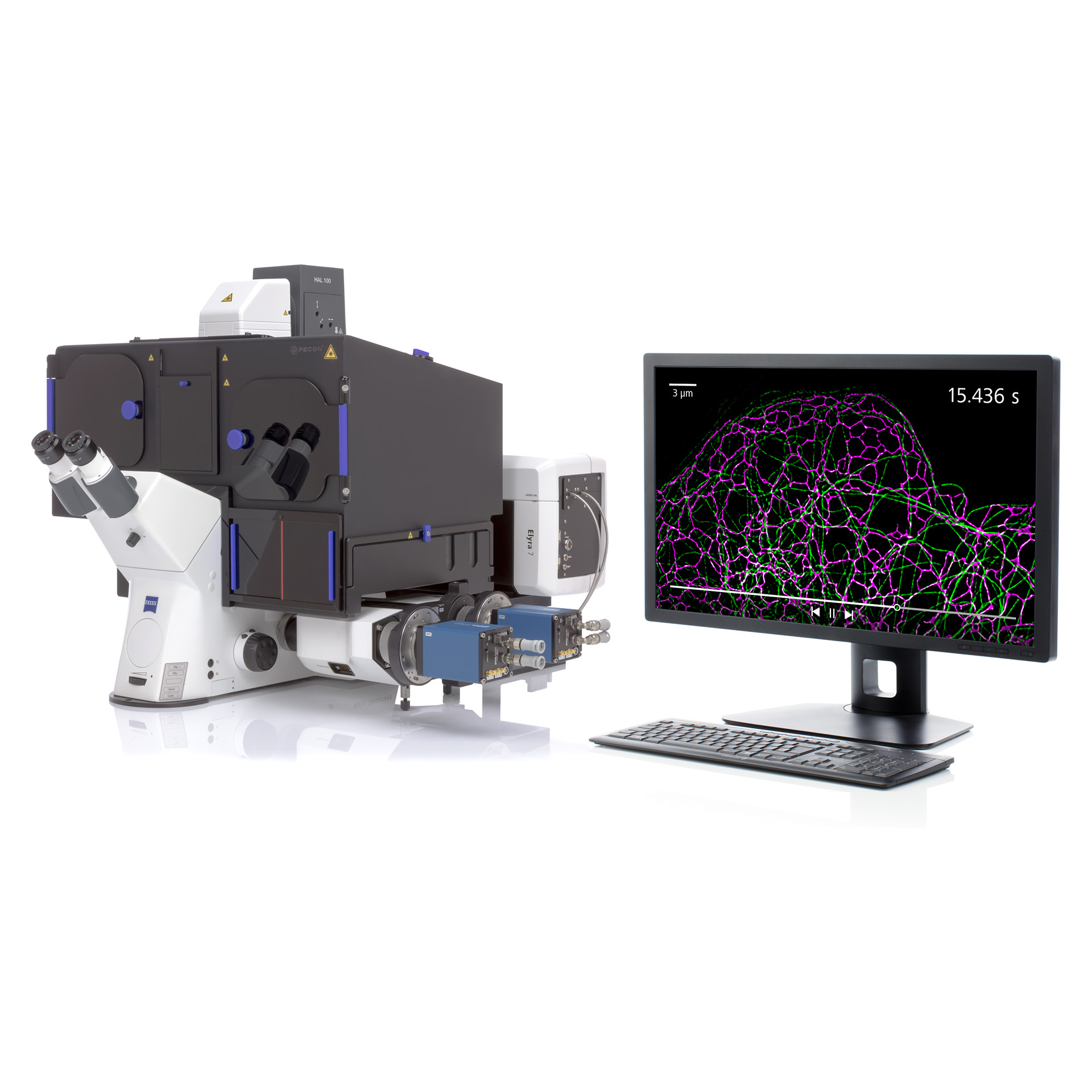

ZEISS Elyra
UK User Group Meeting- 00 years
- 00 months
- 00 days
- 00 hours
- 00 minutes
- 00 seconds

Event Summary
Our upcoming User Group Meeting will bring together selected Elyra Users for the opportunity to share research findings, applications and technology insights. You will be able to meet other ZEISS Elyra users and to hear how they leverage the Elyra for their research purposes.
Over the two days we will have a varied program of informative and practical presentations from users and technical experts. There will be time for Q&A, round table discussions and opportunities for networking.
Event Dates:
- Start Time: 11th January 2024 (11:00)
- End Time: 12th January 2024 (14:00)
Would you like to give a talk at the meeting? Sharing your experience with the Elyra User community is a great way to spread knowledge and gain exposure for the work being done in your lab. We invite you to seize this opportunity by submitting a request to share your recent results with the group during the meeting. Your talk should be a ten minute presentation followed by five minutes for questions. Simply submit your abstract during registration. You will also have the opportunity to suggest topics for discussion when completing the registration form below.
During the meeting you can expect:
- Informative Roundtable Discussions
- Impactful Research Presentations
- Technology Insights From Experts
- Collaboration and Networking Opportunities
Registration is free. The deadline for registration and abstract submission is Monday 18th December 2023.
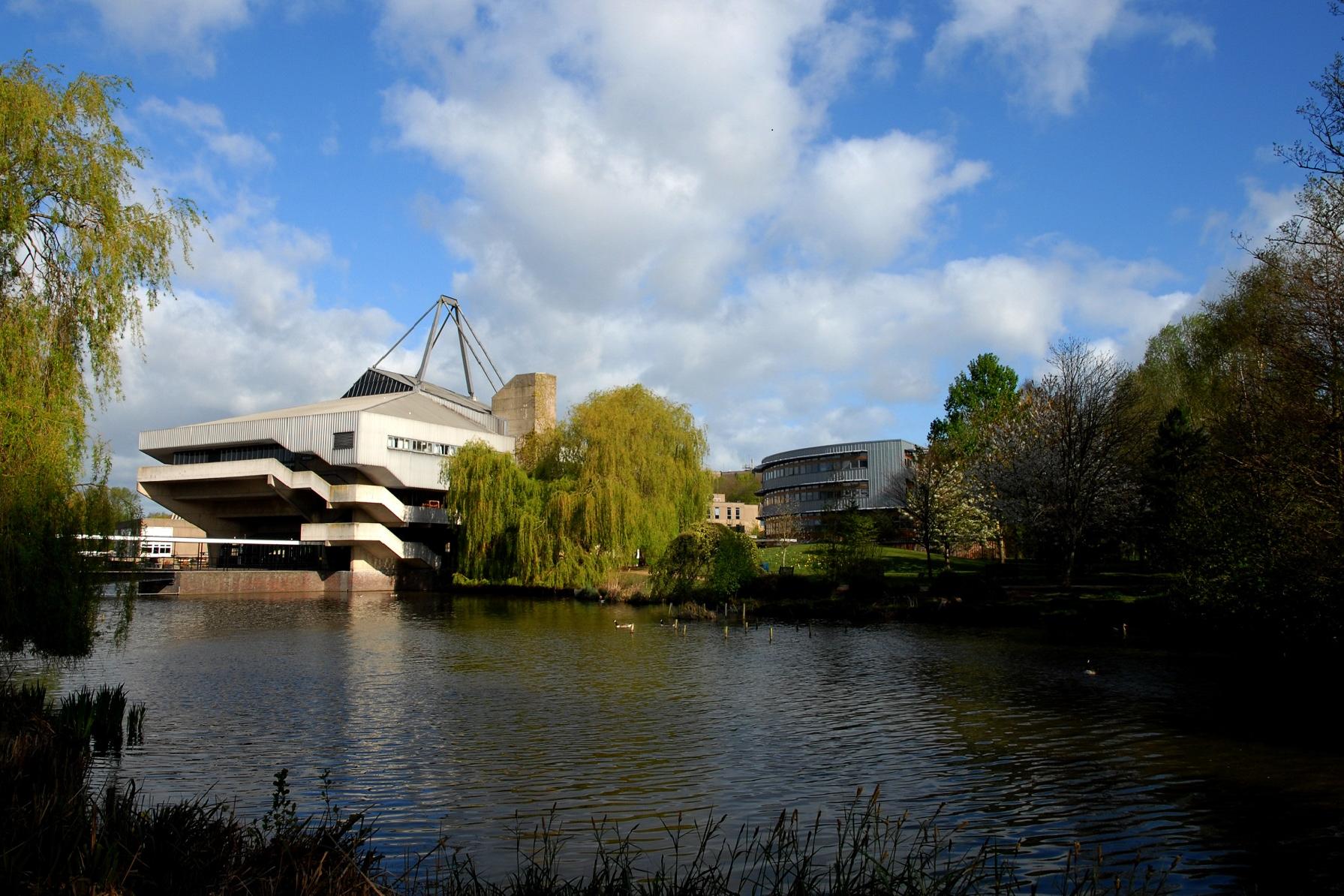
Location & Directions
Bioscience Technology Facility, University of York


Discounted Hotel Rate
Our partners at the University of York have negotiatied a discounted hotel rate at the Hotel Indigo York starting from £96 per night. It is conveniently located located on one of York's oldest streets, in the Walmgate neighbourhood. Click below to take advantage of this special rate and to visit the hotel website for more information.
Address
88 - 96 Walmgate, York, YO1 9TL. United Kingdom
Register To Attend
Complete the form below to book your place. We invite attendees to share their work with other users, simply submit your abstract for consideration when registering via the form below. The deadline for registration and abstract submission is Monday 18th December 2023. Registration is free.
Register
Complete the short form below to register today. We will send additional updates including speaker announcements and other important information to the contact details provided. Registration closes February 12, 2024.


Register To Attend
Complete the form below to book your place. We invite attendees to share their work with other users, simply submit your abstract for consideration when registering via the form below. The deadline for registration and abstract submission is April 14th, 2025. Registration is free.
CD7 User group Liverpool - Form
Agenda
Featured Speakers
We were pleased to have an experienced speaker line up for this meeting. You can expect to hear from speakers who are at the forefront of cutting-edge EM technology in various specialty fields at our future user group meetings. Below we have a selection of featured speaker bios from the event line up.


Dr Alexander Lunt is a Senior Lecturer in Mechanical Engineering at the University of Bath. He is a world leader in micromechanics (90+ publications) with a focus on technique development using microscopy and non-destructive testing. The application base for his work is broad and includes multilayers, composite materials, additively manufactured systems, batteries and more. He has secured substantial funding (£4m+) in collaboration with his extensive academic and industrial research network (GKN, Dowty, Rolls Royce, etc..). Dr Lunt co-directs Bath’s Integrated Materials and Structures research centre and is principal investigator in the University’s collaboration with CERN. Additionally, he is the Imaging and Microscopy user representative at Diamond Light Source, and is Composites Lead Editor for the Elsevier Journal Materials & Design.


Dr. Naresh Gunasekar is a lecturer in compound semiconductor device technology at Cardiff University, leading a research group on developing energy-efficient wide bandgap optical and electronic devices, particularly troubleshooting their reliability issues via correlative micro-spectroscopy. He completed his PhD from Strathclyde University in 2012 on developing and applying “Electron Channelling Contrast Imaging for III-nitride semiconductors” and is currently a fellow of the Royal Microscopical Society.


I’m Eve Burgess, from Oldham in Greater Manchester. I am a second year PhD student at Cardiff University – as part of the EPSRC CDT in Compound Semiconductor Manufacturing- supervised by Dr Juan Pereiro Viterbo, also working closely with the Cardiff University Optoelectronics group. My PhD project is in collaboration with Zeiss to develop a multi-microscopy study of III-V compound semiconductor devices, so far mainly focusing on understanding the reliability of quantum dot (QD) lasers.


Dan is the Market Segment Manager for Materials Analysis at Oxford Instruments, where he was previously a Product Scientist at NanoAnalysis, where he specialised in EBSD and FIB applications. Dan came to Oxford Instruments mid-2022 and was previously a Technical Specialist at Plymouth Electron Microscopy Centre, where he managed their Crossbeam 550. Dan went to Loughborough Uni for both his undergraduate Masters degree and his PhD, both in materials.


Greg has a BS degree from Virginia Tech and performed some graduate research at the University of Florida. At IBM’s Packaging Development Laboratory, he honed his FA skills in packaging, and was soon named an Inventor on 19 US Patents in greensheet formulation and sintering. Then, at IBM’s Semiconductor Research and Development Center, he was either the lead or sole FA engineer for FEOL defect localization across seven, successful, bulk technology node qualifications. And one in SOI. Now at Carl Zeiss Microscopy, he is developing applications in electron and ion microscopy for the semiconductor industry.


Jamie Reynolds is an optical engineer in the Nanophotonics Technology team at Wave Optics / Snap Inc. His background is in nanoelectronics and nanophotonics. He studied at University of Southampton for his PhD in graphene single electron transistors and moved into postdoc researching NEMS and then Silicon photonics before he moved to Wave Optics 3 years ago.


Indraneel Sanyal is currently a Research Associate at the University of Bristol's Centre for Device Thermography and Reliability (CDTR), specializing in the advancement of state-of-the-art Ultrawide bandgap power devices. With a focus on epitaxial growth, Indraneel has dedicated the past eight years to working on ultra/wide bandgap semiconductors such as GaN and Ga2O3, utilizing techniques like molecular beam epitaxy (MBE) and metal organic chemical vapor deposition (MOCVD).
Indraneel's journey began in 2015 at the Indian Institute of Technology, Kharagpur (IITKGP), India, where he developed GaN-on-Si technology using MBE for high-power transistors. From 2016 to 2021, during his Ph.D. in Taiwan, Indraneel played a pivotal role in the design, growth, and characterization of cutting-edge wide bandgap devices including quaternary AlInGaN for GaN-on-Si based RF devices. His contributions extended to technology transfer with the Industrial Technology Research Institute (ITRI), Taiwan, and Lexter.
Acknowledged for excellent graduate research, Indraneel received Taiwan's prestigious CTCI Foundation award in 2020. Actively fostering international collaboration, Indraneel has played a key role in connecting with renowned institutions such as the Tokyo Institute of Technology and the Indian Institute of Technology (Mandi). In Bristol, Indraneel actively engages in grant applications, notably as a Researcher Co-investigator in projects like the EPSRC Horizon with a considerable funding of approximately £200k, focusing on novel van-der-Waal epitaxy of Ga2O3.
Join Us for the 2025 UK EM User Group Meeting!
We are excited to invite you to the second annual UK Electron Microscopy User Group Meeting, tailored exclusively for the UK research community. Following the success of last year’s event, we’re back with an even broader agenda in collaboration with the University of Liverpool.
Why Attend?
This meeting fosters knowledge exchange, expands understanding of materials and electronic components, and introduces cutting-edge technologies in microscopy and multiscale characterization. New for 2025, we’ve incorporated X-Ray Microscopy(XRM) and advanced workflows in response to your valuable feedback.
Event Highlights
- Expert Presentations: Hear from leading researchers and ZEISS experts on topics like lab automation, cryo workflows, FIBSEM workflows, and machine learning applications in materials science.
- Facility Tours: Explore Liverpool’s state-of-the-art SEM and X-Ray Microscopy Shared Research Facilities, featuring instruments like the Gemini 450 FEG SEM and Versa 620.
- Live Demonstrations: Witness ZEISS microscopes in action during remote demos.
- Networking Opportunities: Connect with peers from academia and industry.
What’s in It for You?
- Gain insights into the latest trends and innovations in Electron and X-ray microscopy.
- Engage with a community of materials scientists and industry professionals.
- Learn from real-world applications in 3D imaging, batteries, cement, and beyond.
Event Details
Dates: 26th–27th February 2025
Location: Liverpool Metropolitan Cathedral & University of Liverpool
Agenda: Academic talks, live demos, facility tours, and a community feedback session.
Don’t miss this opportunity to explore cutting-edge research, network with like-minded professionals, and elevate your expertise in materials characterization.
Secure Your Spot Today!
Spaces are limited—register now to be part of what promisies to be a dynamic event!


 illustrate the preparation of an atom probe tomography (APT) sample using ZEISS Crossbeam laser. The sample is silicon. A specific site of the sample was marked by an ion beam induced deposition and prepared. First, a pillar is isolated from the bulk by laser machining. Next, the sample is shaped by FIB milling in steps.")
 illustrate the preparation of an atom probe tomography (APT) sample using ZEISS Crossbeam laser. The sample is silicon. A specific site of the sample was marked by an ion beam induced deposition and prepared. First, a pillar is isolated from the bulk by laser machining. Next, the sample is shaped by FIB milling in steps.")


